
Ethernut 3 Ports
Expansion Port
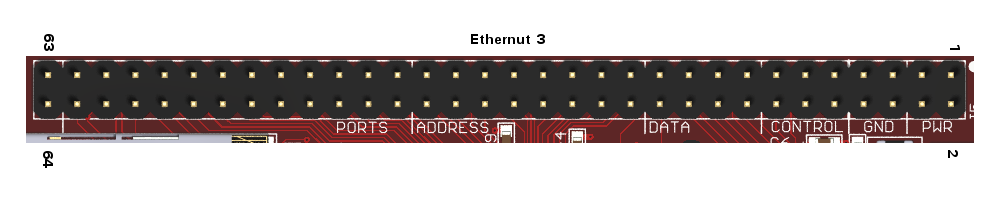
64-Pin Header, 0.05" (2.54 mm) grid, 2 rows
Important note: While all pins on Ethernut 1 are 5V CMOS compatible, and all pins on Ethernut 2 are at least 5V tolerant, the pins on Ethernut 3 are 3.3V. And they are 5V tolerant only, if they are not connected to the CPU. Applying voltages above 3.3V to any CPU pin may destroy the AT91R40008 chip on Ethernut 3.
The Ethernut Expansion Port had been originally specified for the ATmega128. To maintain some compatibility, the AT91 port pins on the Ethernut 3 expansion port are not sorted in a specific order, but follow the AVR functions. In opposite to the AVR, the AT91 ports don't have internal pull-up resistors.
| Pin | Ethernut 3 (ARM7TDMI) | Ethernut 1/2 (AVR) | |||
|---|---|---|---|---|---|
| 1 | VCC3 +3V Power Supply Note 1 | VCC3 +3V Power Supply | |||
| 2 | VCC3 +3V Power Supply Note 1 | VCC3 +3V Power Supply | |||
| 3 | N/C Not Connected | VCC5 +5V Power Supply | |||
| 4 | N/C Not Connected | VCC5 +5V Power Supply | |||
| 5 | GND Digital Ground | GND Digital Ground | |||
| 6 | GND Digital Ground | GND Digital Ground | |||
| 7 | GND Digital Ground | GND Digital Ground | |||
| 8 | GND Digital Ground | GND Digital Ground | |||
| Pin | Ethernut 3 (ARM7TDMI) | Internal Use | CPU | CPLD | Ethernut 1/2 (AVR) |
| 9 | NMR Hardware Reset Input Note 2 | Reset button | 7 | MR\ Hardware Reset Input | |
| 10 | DC Unreg. DC Power Supply Note 3 | DC Unregulated DC Power Supply | |||
| 11 | N/C Not Connected | VCC5 +5V Power Supply | |||
| 12 | N/C Not Connected | VCC5 +5V Power Supply | |||
| 13 | NCRD Configurable Read Strobe | Panel | 57 | RD\ External Memory Bus Read Strobe | |
| 14 | NCWR Configurable Write Strobe | Panel | 58 | WR\ External Memory Bus Write Strobe | |
| Pin | Ethernut 3 (ARM7TDMI) | Internal Use | CPU | CPLD | Ethernut 1/2 (AVR) |
| 15 | CDR0 Configurable Data Bus Bit 0 | Panel | 59 | D0 External Data Bus Bit 0 | |
| 16 | CDR1 Configurable Data Bus Bit 1 | Panel | 60 | D1 External Data Bus Bit 1 | |
| 17 | CDR2 Configurable Data Bus Bit 2 | Panel | 61 | D2 External Data Bus Bit 2 | |
| 18 | CDR3 Configurable Data Bus Bit 3 | Panel | 64 | D3 External Data Bus Bit 3 | |
| 19 | CDR4 Configurable Data Bus Bit 4 | Panel | 66 | D4 External Data Bus Bit 4 | |
| 20 | CDR5 Configurable Data Bus Bit 5 | Panel | 68 | D5 External Data Bus Bit 5 | |
| 21 | CDR6 Configurable Data Bus Bit 6 | Panel | 69 | D6 External Data Bus Bit 6 | |
| 22 | CDR7 Configurable Data Bus Bit 7 | Panel | 70 | D7 External Data Bus Bit 7 | |
| Pin | Ethernut 3 (ARM7TDMI) | Internal Use | CPU | CPLD | Ethernut 1/2 (AVR) |
| 23 | CAR0 Configurable Address Bus Bit 0 | Panel | 71 |
A0 External Address Bus Bit 0 PA0 GPIO Port A Bit 0 |
|
| 24 | CAR1 Configurable Address Bus Bit 1 | Panel | 74 |
A1 External Address Bus Bit 1 PA1 GPIO Port A Bit 1 |
|
| 25 | CAR2 Configurable Address Bus Bit 2 | Panel | 75 |
A2 External Address Bus Bit 2 PA2 GPIO Port A Bit 2 |
|
| 26 | CAR3 Configurable Address Bus Bit 3 | 76 |
A3 External Address Bus Bit 3 PA3 GPIO Port A Bit 3 |
||
| 27 | CAR4 Configurable Address Bus Bit 4 | 77 |
A4 External Address Bus Bit 4 PA4 GPIO Port A Bit 4 |
||
| 28 | CAR5 Configurable Address Bus Bit 5 | 78 |
A5 External Address Bus Bit 5 PA5 GPIO Port A Bit 5 |
||
| 29 | CAR6 Configurable Address Bus Bit 6 | 79 |
A6 External Address Bus Bit 6 PA6 GPIO Port A Bit 6 |
||
| 30 | CAR7 Configurable Address Bus Bit 7 | 80 |
A7 External Address Bus Bit 7 PA7 GPIO Port A Bit 7 |
||
| 31 | CAR8 Configurable Address Bus Bit 8 | 81 |
A8 External Address Bus Bit 8 PC0 GPIO Port C Bit 0 |
||
| 32 | CAR9 Configurable Address Bus Bit 9 | 82 |
A9 External Address Bus Bit 9 PC1 GPIO Port C Bit 1 |
||
| 33 | CAR10 Configurable Address Bus Bit 10 | 83 |
A10 External Address Bus Bit 10 PC2 GPIO Port C Bit 2 |
||
| 34 | CAR11 Configurable Address Bus Bit 11 | 85 |
A11 External Address Bus Bit 11 PC3 GPIO Port C Bit 3 |
||
| 35 | CAR12 Configurable Address Bus Bit 12 | 86 |
A12 External Address Bus Bit 12 PC4 GPIO Port C Bit 4 |
||
| 36 | CAR13 Configurable Address Bus Bit 13 | 87 |
A13 External Address Bus Bit 13 PC5 GPIO Port C Bit 5 |
||
| 37 | CAR14 Configurable Address Bus Bit 14 | 88 |
A14 External Address Bus Bit 14 PC6 GPIO Port C Bit 6 |
||
| 38 | CAR15 Configurable Address Bus Bit 15 | 91 |
A15 External Address Bus Bit 15 PC7 GPIO Port C Bit 7 |
||
| Pin | Ethernut 3 (ARM7TDMI) | Internal Use | CPU | CPLD | Ethernut 1/2 (AVR) |
| 39 |
P15 GPIO Port Bit 15 Note 4 RXD0 UART 0 Receive Input |
RS232 | 69 | 92 |
PE0 GPIO Port E Bit 0 RXD0 UART 0 Receive Input PDI Programming Data Input |
| 40 |
P14 GPIO Port Bit 14 TXD0 UART 0 Transmit Output |
RS232 | 68 | 93 |
PE1 GPIO Port E Bit 1 TXD0 UART 0 Transmit Output PDO Programming Data Output |
| 41 |
P13 GPIO Port Bit 13 SCK0 USART 0 External Clock |
67 | 94 |
PE2 GPIO Port E Bit 2 XCK0 USART 0 External Clock AIN0 Analog Comparator Positive Input |
|
| 42 |
P8 GPIO Port Bit 8 TIOB2 Counter Channel 2 I/O Pin B |
59 | 95 |
PE3 GPIO Port E Bit 3 OC3A Counter 3 Compare and PWM A AIN1 Analog Comparator Positive Input |
|
| 43 |
P9 GPIO Port Bit 9 Note 5 IRQ0 External Interrupt Request 1 |
CPLD IRQ | 60 | 96 |
PE4 GPIO Port E Bit 4 INT4 External Interrupt 4 OC3B Counter 3 Compare and PWM B |
| 44 |
P27 GPIO Port Bit 27 NCS3 Chip Select 3 Note 6 |
100 | 97 |
PE5 GPIO Port E Bit 5 INT5 External Interrupt 5 OC3C Counter 3 Compare and PWM C |
|
| 45 |
P11 GPIO Port Bit 11 IRQ2 External Interrupt Request 2 |
64 |
PE6 GPIO Port E Bit 6 INT6 External Interrupt 6 T3 Counter 3 Clock Input |
||
| 46 |
P12 GPIO Port Bit 12 FIQ Fast Interrupt Request |
66 | 98 |
PE7 GPIO Port E Bit 7 INT7 External Interrupt 7 ICP3 Counter 3 Input Capture |
|
| 47 |
P0 GPIO Port Bit 0 TCLK0 External Clock Counter Channel 0 |
49 |
PB0 GPIO Port B Bit 0 -SS SPI Slave Select Input |
||
| 48 |
P1 GPIO Port Bit 1 TIOA0 Counter Channel 0 I/O Pin A |
50 |
PB1 GPIO Port B Bit 1 SCK SPI Bus Serial Clock |
||
| 49 |
P2 GPIO Port Bit 2 TIOB0 Counter Channel 0 I/O Pin B |
51 |
PB2 GPIO Port B Bit 2 MOSI SPI Bus Master Output / Slave Input |
||
| 50 |
P3 GPIO Port Bit 3 TCLK1 External Clock Counter Channel 0 |
54 | 100 |
PB3 GPIO Port B Bit 3 MISO SPI Bus Master Input / Slave Output |
|
| 51 |
P4 GPIO Port Bit 4 TIOA1 Counter Channel 1 I/O Pin A |
55 | 101 |
PB4 GPIO Port B Bit 4 OC0 Counter 0 Compare and PWM |
|
| 52 |
P5 GPIO Port Bit 5 TIOB1 Counter Channel 1 I/O Pin B |
56 | 102 |
PB5 GPIO Port B Bit 5 OC1A Counter 1 Compare and PWM A |
|
| 53 |
P6 GPIO Port Bit 6 TCLK2 External Clock Counter Channel 0 |
57 | 103 |
PB6 GPIO Port B Bit 6 OC1B Counter 1 Compare and PWM B |
|
| 54 |
P7 GPIO Port Bit 7 TIOA2 Counter Channel 2 I/O Pin A |
58 | 104 |
PB7 GPIO Port B Bit 7 OC1C Counter 1 Compare and PWM C OC2 Counter 2 Compare and PWM |
|
| Pin | Ethernut 3 (ARM7TDMI) | Internal Use | CPU | CPLD | Ethernut 1/2 (AVR) |
| 55 | P17 GPIO Port Bit 17 Note 7 | I2C SCL | 71 | 105 |
PD0 GPIO Port D Bit 0 INT0 External Interrupt 0 SCL TWI Serial Clock |
| 56 | P16 GPIO Port Bit 16 Note 7, 8 | I2C SDA XTMS (JP9) | 70 | 106 |
PD1 GPIO Port D Bit 1 INT1 External Interrupt 1 SDA TWI Serial Data |
| 57 |
P22 GPIO Port Bit 22 Note 4 RXD1 UART 1 Receive Input |
(RS232) | 76 | 107 |
PD2 GPIO Port D Bit 2 INT2 External Interrupt 2 RXD1 UART 1 Receive Input |
| 58 |
P21 GPIO Port Bit 21 TXD1 UART 1 Transmit Output NTRI Three-State Mode Select |
(RS232) | 75 | 110 |
PD3 GPIO Port D Bit 3 INT3 External Interrupt 3 TXD1 UART 1 Transmit Output |
| 59 | P23 GPIO Port Bit 23 Note 8 | XTDI (JP9) | 83 | 111 |
PD4 GPIO Port D Bit 4 ICP1 Counter 1 Input Capture |
| 60 |
P20 GPIO Port Bit 20 SCK1 USART 1 External Clock |
74 | 112 |
PD5 GPIO Port D Bit 5 XCK1 USART 1 External Clock |
|
| 61 | P19 GPIO Port Bit 19 Note 8 | XTDO (JP9) | 73 | 113 |
PD6 GPIO Port D Bit 6 T1 Counter 1 Clock Input |
| 62 | P18 GPIO Port Bit 18 Note 8 | XTCK (JP9) | 72 | 115 |
PD7 GPIO Port D Bit 7 T2 Counter 2 Clock Input |
| 63 | N/C Not Connected Note 9 | N/C Not Connected | |||
| 64 | N/C Not Connected Note 9 |
N/C if R34 not mounted ALE External Address Bus Latch Enable |
|||
Note 1
External expansion boards may draw up to 300 mA from
the Ethernut 3.3V supply.
Note 2
Pin 9 can be used to reset Ethernut when connected to an open
collector output or an external push button.
Note 3
Pin 10 is connected to the power supply input of the Ethernut
board. However, it is not directly connected but routed through
the rectifier bridge and protected by a Transil Diode against
overvoltage (> 24V) and a 1A fast acting fuse. The rectifier
bridge has a very low voltage drop of typically 1V only. Up to
1A may be drawn by the Ethernut board plus expansion hardware.
This pin may also be used to provide power supply for the
Ethernut board. In this case keep the voltage between 6 and
24 Volts. The Ethernut Board will draw about 200 mA at 6V,
100 mA at 12V or 50 mA at 24V.
Note 4
Using pin 39 (P15) or pin 57 (P22) as GPIO requires CPLD
re-programming.
Note 5
Pin 43 (P9) is used by the CPLD for interrupt request.
Using this pin for GPIO requires CPLD re-programming.
Note 6
Using pin 44 for chip select requires a modified memory
remapping in the C startup file.
Note 7
Pins 55 (SCL) and 56 (SDA) are used to control the two
on-board I2C devices, the programmable PLL clock and the
RTC/EEPROM chip. External I2C hardware (3.3V) can be
additionally attached to these pins.
Pin 55 (P17) should not be used as GPIO. If I2C is idle
(pin 55 always high), then pin 56 (P16) may be used as a
limited input pin. Note, that both pins have pull up
resistors attached.
Note 8
Pins 56 (P16), 59 (P23), 61 (P19) and 62 (P18) are used
as TMS, TDI, TDO and TCK resp. during CPLD programming
with the XSVF Executor Utility. Make sure to disconnect
them from the CPLD JTAG via JP9, before using them as
outputs.
Note 9
Pins 63 and 64 are reserved for custom applications
and will be kept unconnected throughout all Ethernut
revisions.
Panel Connector
24-Pin Flat Cable Connector, 0.5 mm Pitch
The panel connector can be used to attach a front panel board, containing LCD, keyboard or similar user interfaces. It contains an 8 bit data bus, a 3 bit address bus as well as a read and a write strobe line, which are all shared with the same lines at the expansion bus. In addition there is a dedicated panel chip select line. Last not least a 3.3V power supply is available.
This connector is not available on Ethernut 1 and 2.
| Pin | Signal | CPLD |
|---|---|---|
| 1 | VCC3 +3.3V Power Supply | |
| 2 | GND Digital Ground | |
| 3 | CDR7 Configurable Data Bus Bit 7 | 70 |
| 4 | CDR6 Configurable Data Bus Bit 6 | 69 |
| 5 | GND Digital Ground | |
| 6 | CDR5 Configurable Data Bus Bit 5 | 68 |
| 7 | CDR4 Configurable Data Bus Bit 4 | 66 |
| 8 | GND Digital Ground | |
| 9 | CDR3 Configurable Data Bus Bit 3 | 64 |
| 10 | CDR2 Configurable Data Bus Bit 2 | 61 |
| 11 | GND Digital Ground | |
| 12 | CDR1 Configurable Data Bus Bit 1 | 60 |
| 13 | CDR0 Configurable Data Bus Bit 0 | 59 |
| 14 | GND Digital Ground | |
| 15 | NCWR Configurable Write Strobe | 58 |
| 16 | NCRD Configurable Read Strobe | 57 |
| 17 | GND Digital Ground | |
| 18 | PNCS Configurable Panel Chip Select | 56 |
| 19 | CAR0 Configurable Address Bus Bit 0 | 71 |
| 20 | GND Digital Ground | |
| 21 | CAR1 Configurable Address Bus Bit 1 | 74 |
| 22 | CAR2 Configurable Address Bus Bit 2 | 75 |
| 23 | GND Digital Ground | |
| 24 | VCC3 +3.3V Power Supply |
Except ground and power supply, all lines at the panel connector are 5V tolerant and re-configurable by replacing the CPLD contents.
MMC Socket
Low Profile SD Card Socket
The MMC Socket can be used for Multimedia and Secure Digital Cards. Currently Nut/OS supports SPI Mode only.
Ethernut 1 and 2 don't provide any card socket. Instead, a 20-pin header at the same board location offers an 8 channel ADC. In turn, Ethernut 3 doesn't provide analog inputs.
| Pin | Signal | SPI Mode | 4-Bit SD Mode | CPLD |
|---|---|---|---|---|
| 1 | MDAT3 | Card Select | Bidirectional Data Line 3 | 128 |
| 2 | MCMD | Serial Data Output Line | Bidirectional Command/Response Line | 126 |
| 3 | GND | Digital Ground | ||
| 4 | VCC3 | +3.3V Power Supply | ||
| 5 | MCLK | Clock Output | 125 | |
| 6 | GND | Digital Ground | ||
| 7 | MDAT0 | Serial Data Input Line | Bidirectional Data Line 0 | 124 |
| 8 | MDAT1 | Interrupt Line | Bidirectional Data Line 1 | 121 |
| 9 | MDAT2 | Not Used | Bidirectional Data Line 2 | 129 |
| C | GND | Digital Ground | ||
| WP | MWP | Write Protect Sense | 130 | |
| CD | MCD | Card Detect Sense | 120 | |
RS232 Connector
9-pin female DB-9 connector.
Ethernut 3 uses a male DB-9 connector with full modem handshake, in opposite to Ethernut 1 and 2, which both provide a female type with no or RTS/CTS flow control only.
| Pin | Signal | CPLD |
|---|---|---|
| 1 | DCD Data Carrier Detect Input | 48 CDCD |
| 2 | RD Receive Data Input | 45 CRD |
| 3 | TD Transmit Data Output | 41 CTD |
| 4 | DTR Data Terminal Ready Output | 40 CDTR |
| 5 | GND | |
| 6 | DSR Data Set Ready Input | 46 CDSR |
| 7 | RTS Request To Send Output | 43 CRTS |
| 8 | CTS Clear To Send Input | 44 CCTS |
| 9 |
RI Ring Indicator Input, if R1 mounted (default) |
49 CRI |
Ethernet Connector
8-pin RJ-45 connector with integrated LEDs and transformer.
Ethernut 3 does not support power supply over Ethernet. Compared to Ethernut 1 and 2, LED colors had been swapped. The green LED signals link and the yellow LED lits on activity.
| Pin | Signal |
|---|---|
| 1 | TX+ Positive Transmit Line |
| 2 | TX- Negative Transmit Line |
| 3 | RX+ Positive Receive Line |
| 4/5 | Connected to shield via 75 Ohm / 10 nF |
| 6 | RX- Negative Receive Line |
| 7/8 | Connected to shield via 75 Ohm / 10 nF |
Power Supply Connector
2.0 mm barrel connector.
Due to the on-board rectifier bridge, polarity doesn't matter.