
Ethernut 3 JTAG
During the development phase it is recommended to use the TFTP based bootloader for Ethernut 3, which is much faster than any other method to upload the compiled code from the PC into the Ethernut 3 RAM.
JTAG programming is required to initially burn the bootloader into flash memory or to permanently store application code.
Beginners may first get confused, because JTAG had been specified by the Joint Test Action Group (see logo) for testing electronic boards using boundary scan. Today it is also widely used for software debugging, which includes uploading and downloading (programming) of memory contents.
The IEEE Std 1149.1 (JTAG) Testability Primer from Texas Instruments provides a good introduction to JTAG.
JTAG Signals
Only four core signals are required to meet the initial IEEE Std 1149.1-1990.
TCK from adapter to target
The test clock signal is used to clock in and clock out the test data, which is sampled on the TCK rising edge. Typically a 10kOhm pull-up is used on the target.TMS from adapter to target
The test mode select input of the target's TAP controller is used to select the state machine path on each clock cycle. Typically a 10kOhm pull-up is used on the target.TDI from adapter to target
The serial test data input of the target's TAP controller. Typically a 10kOhm pull-up is used on the target.TDO from target to adapter
The serial test data output of the target's TAP controller. Sometimes a 33 Ohm series resistor is used on the target.
The following lines are optional. Some of them are useful and some are required by specific targets.
RTCK from target to adapter
Some chips are entirely controlled by a single clock, where TDO changes are possibly asynchronous to TCK. The re-synchronized RTCK can be used by the JTAG adapter to deal with asynchronous TDO signals. The adapter will not change TCK until it gets back the RTCK edge from a previous TCK change. This results in a second advantage, because the adapter can dynamically adapt the JTAG clock rate to the target's ability. If, for example, the target is switched to sleep mode and running on a reduced main clock, it may not be able to handle full speed JTAG clocking.nSRST bi-directional (open collector)
This pin serves two purposes. It can be used by the adapter to reset the target board, which is most useful during remote debugging. Furthermore, the adapter is able to detect that the reset is triggered on the target by another event, like pressing the reset button or a watchdog timeout.nTRST from adapter to target
According to the JTAG standard, the TAP controller is reset to a known state by keeping TMS high for five consecutive TCK cycles. However, some targets have problems with this sequence and thus require a hardware reset, which is marked optional in the IEEE specification. On several chips, like the AT91R40008 used on Ethernut 3, nSRST and nTRST are internally tied together. The disadvantage with this design is, that you can't trigger a breakpoint immediately after a target hardware reset. If this signal is not used on the target, it is recommended to pull up this line with 10kOhm.DBGRQ from adapter to target
This pin allows to quickly enter debug mode and is used by some logic analyzers for advanced breakpoint settings. Normally scan chain 2 is used to put the target in debug state. If breakpoints must be triggered on external events, using the scan chain is ususally too slow.DBGACK from target to adapter
This pin allows an external logic analyzer to quickly determine whether the target is in debug mode or not. If this pin is not available, the debug state can be determined only by continously polling scan chain 2, which is much slower. On some targets this line is permanently pulled low.VTref target logic level reference
This pin is usually tied to the target's power supply and used by the adapter as a logic level reference.Vsupply adapter supply from target
This pin may be used by the adapter to draw its power supply from the target. Not all targets may provide this option, e.g. when driven from batteries. The target's supply voltage may also be too low to drive the adapter. Also note, that Vsupply may provide a higher voltage than VTref.
Programming Hardware
The standard JTAG adapter for Ethernut 3 is the Turtelizer 2, which is used with OpenOCD. Ready-to-use devices are available from www.egnite.de.
In fact, any JTAG adapter for the ARM7TDMI may be used, but the connector layout on Ethernut 3 is kind of alien in the world of ARM CPUs. See the next chapter.
The most simple adapter for the PC's parallel printer port, a so called Wiggler compatible adapter can be easily built without much effort. A sample schematic is available at jtag-arm9.sourceforge.net. However, this one uses a 74AC244 buffer and may not work reliable with 3.3V targets like Ethernut 3. When driven by a 3.3V power supply, the lines from the parallel port may raise above Vcc + 0.5, which violates the absolute maximum ratings given in the datasheet. In the worst case, voltages above 3.3V may appear on the target side of the JTAG adapter and destroy the target board. The 5V tolerant versions 74LVC244 or 74LVX244 are better choices, but are available as SMD parts only, requiring some soldering skills. As an alternative you can use the 74HC244 and add 220 Ohm series resistors between the chip inputs and the parallel port outputs. Internal diodes clamp the voltage at the inputs and the series resistors will limit the resulting current.

The original Wiggler shown above can be purchased from
www.macraigor.com. It comes with software, which
supports a large number of target devices.
A not so simple adapter is the Turtelizer 1, which was included in early Ethernut 3 Starter Kits from www.egnite.de. The hardware is actually based on a modified SP Duo Adapter, which is a commercial product developed by Embedded Creations for the AVR. With minimal AVR experience, it should not be too difficult to re-program the SP Duo 2 or build to a similar board, if you want to. In general the Turtelizer 1 contains an ATmega8L and an RS232 level shifter.
Of course, an Ethernut 1 or 2 may be used to run the Turtelizer 1 firmware and make nice JTAG adapter, although a bit expensive.
Ethernut Connector And De-Facto Standards
On all Ethernut Boards the same connector layout is used for JTAG, which is the same as the one used by Atmel for the AVR and which is used by most AVR based boards.
| Ethernut 10-Pin JTAG Connector | |
|---|---|
| TCK - 1 | 2 - GND |
| TDO - 3 | 4 - VTref |
| TMS - 5 | 6 - nSRST |
| Vsupply - 7 | 8 - NC |
| TDI - 9 | 10 - GND |
A similar layout is used by Altera.
However, most ARM based boards use a different connector, either with 14 or 20 pins. You can still use a programmer with one of these connectors, but a cable adapter will be needed.
Additional ground wires at the 14-pin connector allow higher transfer rates on longer cables.
| Standard 14-Pin JTAG Connector | |
|---|---|
| VTref - 1 | 2 - GND |
| nTRST - 3 | 4 - GND |
| TDI - 5 | 6 - GND |
| TMS - 7 | 8 - GND |
| TCK - 9 | 10 - GND |
| TDO - 11 | 12 - nSRST |
| VTref - 13 | 14 - GND |
The 20-pin connector designed by ARM offers three additional control lines (RTCK, DBGRQ and DBGACK) including additional ground lines for better signal integrity. Today this is the most common JTAG connector layout for ARM CPUs.
Typically a dual row pin header with 0.1" or 0.05" pitch is used, either vertical or angled.
| Standard 20-Pin JTAG Connector | |
|---|---|
| VTref - 1 | 2 - Vsupply |
| nTRST - 3 | 4 - GND |
| TDI - 5 | 6 - GND |
| TMS - 7 | 8 - GND |
| TCK - 9 | 10 - GND |
| RTCK - 11 | 12 - GND |
| TDO - 13 | 14 - GND |
| nSRST - 15 | 16 - GND |
| DBGRQ - 17 | 18 - GND |
| DBGACK - 19 | 20 - GND |
For real-time tracing additional signal lines may be required. For the ARM Embedded Trace Macrocell a 38-pin connector is recommended, which combines an ETM trace port with a JTAG interface.
| 38-Pin AMP Mictor Connector | |
|---|---|
| N/C - 1 | 2 - N/C |
| N/C - 3 | 4 - N/C |
| GND - 5 | 6 - TRACECLK |
| DBGRQ - 7 | 8 - DBGACK |
| nSRST - 9 | 10 - EXTTRIG |
| TDO - 11 | 12 - Vtref |
| RTCK - 13 | 14 - Vsupply |
| TCK - 15 | 16 - TRACEPKT[7] |
| TMS - 17 | 18 - TRACEPKT[6] |
| TDI - 19 | 20 - TRACEPKT[5] |
| nTRST - 21 | 22 - TRACEPKT[4] |
| TRACEPKT[15] - 23 | 24 - TRACEPKT[3] |
| TRACEPKT[14] - 25 | 26 - TRACEPKT[2] |
| TRACEPKT[13] - 27 | 28 - TRACEPKT[1] |
| TRACEPKT[12] - 29 | 30 - TRACEPKT[0] |
| TRACEPKT[11] - 31 | 32 - TRACESYNC |
| TRACEPKT[10] - 33 | 34 - PIPESTAT[2] |
| TRACEPKT[9] - 35 | 36 - PIPESTAT[1] |
| TRACEPKT[8] - 37 | 38 - PIPESTAT[0] |
Programming Software
Any programming software with ARM7TDMI support may be used.
Some years ago, the situation for Open Source Software was dissatisfactory. Either a specific tool was not available for Linux, OS X or Win32 or never has been finished or was too specific towards a special programmer or target. Or it simply didn't work. So we decided to create a separate Project at SourceForge, called JTAG-O-MAT.
This utility is far from being perfect, but the full source code is provided and it works half-way reliable for Ethernut 3 with the Turtelizer 1 (on Linux and Win32) or the Wiggler programming adapters (currently Win32 only).
Then Dominic Rath jumped in and created Openocd as part of a diploma thesis at the University of Applied Sciences, FH-Augsburg. While OpenOCD will work with Turtelizer 1, a new Turtelizer 2 had been developed to specifically support Ethernut 3 programming and debugging via USB. Even the old JTAG-O-MAT utility had been updated to work with Turtelizer 2. The funny thing is, that this version connects to OpenOCD, which needs to be running in the background.
Restoring the Bootloader
If the bootloader is destroyed by accident or if you need to replace it with a different version, you can use the OpenOCD utility. A special Win32 version is available on the download page. You'll find version for Linux and Mac OS X on several other websites.
You additionally need to download the bootloader code.
bootmon-1.2.1.zip
contains the source code as well as a pre-compiled binary. Best
unpack it in your Nut/OS application directory, the sample
directory created by the Nut/OS Configurator. However, any other
place will be OK too.
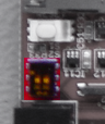
Connect the Turtelizer 2 programming adapter to any USB port of your PC and connect the flat cable with the 10-pin JTAG connector of your Ethernut 3 board. Make sure that the JTAG jumper on the Ethernut Board is configured for programming the AT91 CPU as shown in the following image. Finally switch on the Ethernut 3 power supply.

OpenOCD is a command line driven tool. A file named burn.cmd is included in the archive and has been prepared to upload code to the Ethernut 3 Flash memory. The latter is the right one for the boot loader. To upload the bootloader, change to the directory that contains the bootmon.hex file.
cd bootmon
SET PATH=C:\ethernut\nut\tools\win32;%PATH%
On Linux it is typically not required to extend the PATH environment. After installation the executable will be typically stored in /usr/local/bin/ and the other files in /usr/local/etc/.
Now enter the following OpenOCD programming command sequence
openocd -s /ethernut/nut/tools/turtelizer2 \
 -c "source [find interface/turtelizer2.cfg]" \
 -c "source [find board/ethernut3.cfg]" \
 -c init -c "reset init" \
 -c "flash write_image erase ./bootmon.hex 0 ihex" \
 -c "verify_image ./bootmon.hex 0 ihex" \
 -c reset \
 -c shutdown
or simply
burn
on your Windows PC.
If everything works as expected, the following output should appear
Open On-Chip Debugger 0.4.0-rc1 (2010-02-02-07:03)
For bug reports, read
        http://openocd.berlios.de/doc/doxygen/bugs.html
srst_only srst_pulls_trst srst_gates_jtag srst_open_drain
jtag_nsrst_delay: 300
jtag_ntrst_delay: 300
fast memory access is enabled
dcc downloads are enabled
16000 kHz
Info : device: 4 "2232C"
Info : deviceID: 67354056
Info : SerialNumber: TLQQMFPLA
Info : Description: Turtelizer JTAG/RS232 Adapter A
Info : clock speed 6000 kHz
Info : JTAG tap: at91r40008.cpu tap/device found: 0x1f0f0f0f (mfg: 0x787, part: 0xf0f0, ver: 0x1)
Info : Embedded ICE version 1
Info : at91r40008.cpu: hardware has 2 breakpoints or watchpoints
Info : JTAG tap: at91r40008.cpu tap/device found: 0x1f0f0f0f (mfg: 0x787, part: 0xf0f0, ver: 0x1)
Warn : srst pulls trst - can not reset into halted mode. Issuing halt after reset.
target state: halted
target halted in Thumb state due to debug-request, current mode: Supervisor
cpsr: 0x400000f3 pc: 0x10001698
Info : Flash Manufacturer/Device: 0x001f 0x00c8
flash 'cfi' found at 0x10000000
auto erase enabled
wrote 7672 byte from file ./bootmon.hex in 0.255014s (29.380 kb/s)
verified 7672 bytes in 0.071004s (105.518 kb/s)
Info : JTAG tap: at91r40008.cpu tap/device found: 0x1f0f0f0f (mfg: 0x787, part: 0xf0f0, ver: 0x1)
If something went wrong, please refer to the OpenOCD manual.
Flashed Applications
When an application has been tested, you may want to flash it into Ethernut's non-volatile memory, so it boots up every time power is applied or reset is pressed.
The first thing that needs to be done is to change the default setting of your build tree. Start the configurator and change the linker script from at91_ram to at91_boot.

Then rebuild the build tree, create the sample tree again and then build your application, in this order. The second step is required to update the Makefiles. It will not touch any existing application source code.
We can use the same command as with the bootloader to burn the application's binary image into flash memory
openocd -s /ethernut/nut/tools/turtelizer2 \
 -c "source [find interface/turtelizer2.cfg]" \
 -c "source [find board/ethernut3.cfg]" \
 -c init -c "reset init" \
 -c "flash write_image erase ./httpserv.hex 0 ihex" \
 -c reset \
 -c shutdown
Note, that this application binary will no longer run, if directly uploaded into RAM. The at91_boot linker script will implement a different runtime initialization, which copies the code from Flash Memory to RAM. Thus, the code is still executed at full speed in the 32 bit internal RAM and still limited to 256 kBytes total memory for code and data.
When using the at91_bootcrom linker script, the code is also copied to and running in RAM. But all constants remain in Flash memory. This is useful for large UROM file systems or similar large areas of constant data.
The at91_rom linker script can be used for large programs, where program code directly runs in Flash memory. Programs may grow upto 4 MBytes, leaving the entire 256 kBytes of RAM available for variables.
Flash Memory Layout
As explained in Ethernut 3 Memory Map, after system reset the flash memory is located at address 0x00000000 and will be remapped later to 0x10000000. This remapping is done by the bootloader or may be done via JTAG before uploading the application code into RAM.
Beside that, Ethernut 3 contains a tiny double slide switch, located between the JTAG connector and the reset button. This slide switch divides the 4 MByte flash memory chip into four pages.
As shown in the schematic, the switch selects either the original or the negated signal of address bits 20 and 21. This way the following absolute flash memory addresses are moved the CPU address space (after remap):

| SW A20 | SW A21 | Chip Address | CPU Address |
|---|---|---|---|
| Ori | Ori |
0x00000000 0x00100000 0x00200000 0x00300000 |
0x10000000 0x10100000 0x10200000 0x10300000 |
| Neg | Ori |
0x00100000 0x00000000 0x00300000 0x00200000 |
0x10000000 0x10100000 0x10200000 0x10300000 |
| Ori | Neg |
0x00200000 0x00300000 0x00000000 0x00100000 |
0x10000000 0x10100000 0x10200000 0x10300000 |
| Neg | Neg |
0x00300000 0x00200000 0x00100000 0x00000000 |
0x10000000 0x10100000 0x10200000 0x10300000 |
The address line is negated, if the slide switch is moved towards the reset switch and not negated if moved towards the JTAG connector. The slider at the edge of the board is the one that switches address bit 20.
Note:
When programming the Flash memory, make sure that the slide switches
are in their default positions. The AT49BV322A Flash chip
used on Ethernut 3 has 63 pages of 64 kBytes and 16 pages of 8 kBytes.
The latter are located at chip relative addresses 0x00000000 to 0x0001FFFF.
Thus the smaller pages move when changing the slide switch settings.
This will confuse the programming software.